
クイックステップ™ SCM
信号対雑音比を改善するために、従来のSCMは非常に遅い速度を採用することで、検出器がデータを収集するための十分な時間を設けています。クイックステップ™ SCMは、従来の低速連続移動とは異なる方法を採用しております。データを記録するためにXYスキャナーが各ピクセルポイントで止まり、次の測定ポイントに高速かつ迅速に移ります。これにより、従来のSCMによる低速測定と同じ信号感度を維持しながら、スキャン速度を効果的に高速化できます。

信号対雑音比を改善するために、従来のSCMは非常に遅い速度を採用することで、検出器がデータを収集するための十分な時間を設けています。クイックステップ™ SCMは、従来の低速連続移動とは異なる方法を採用しております。データを記録するためにXYスキャナーが各ピクセルポイントで止まり、次の測定ポイントに高速かつ迅速に移ります。これにより、従来のSCMによる低速測定と同じ信号感度を維持しながら、スキャン速度を効果的に高速化できます。
With the implementation of QuickStep Scan, the throughput of the Scanning Capacitance Microscopy (SCM) measurement was dramatically increased, as much as ten times the standard SCM scan speeds, without compromising signal sensitivity, spatial resolution or data accuracy. In QuickStep scan, the XY scanner stops at each pixel point to record the data, and it makes a fast jump between the pixel points.
Scanning Capacitance Microscopy (SCM) images spatial variations in capacitance. One of the most common applications of SCM is mapping of the carrier concentration on the non-uniformly doped samples.
In semiconductor manufacturing, the ability to characterize the dopant profile is important in identifying causes of failure as well as in making design advancements.
For device characterization, SCM provides the unique ability to measure quantitative 2D dopant profiles.
The SCM consists of a conductive metal probe tip and a highly sensitive capacitance sensor in addition to the normal Atomic Force Microscopy (AFM) components. Like Electrostatic Force Microscopy (EFM), SCM applies a voltage between the tip and the sample as in Metal-Oxide-Semiconductor (MOS) structures.
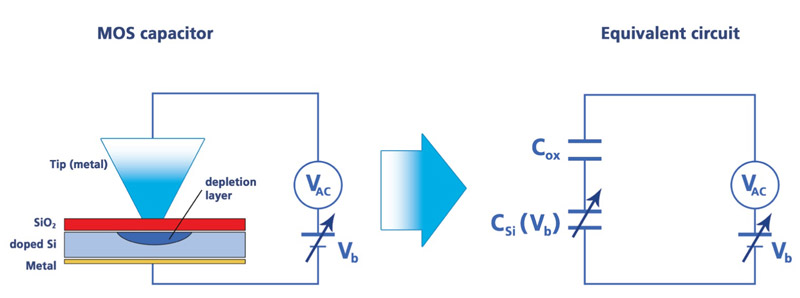
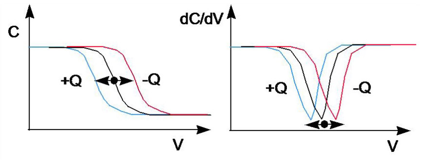
The total capacitance is determined by the oxide thickness and the thickness of depletion layer which depends on the carrier concentration in the silicon substrate and the applied DC voltage between the tip and the semiconductor. The applied AC bias voltage produces capacitance variation at fixed DC bias. The SCM detects differential capacitance (dC/dV) at fixed DC and AC bias voltage as the tip moves across different regions in carrier concentration.
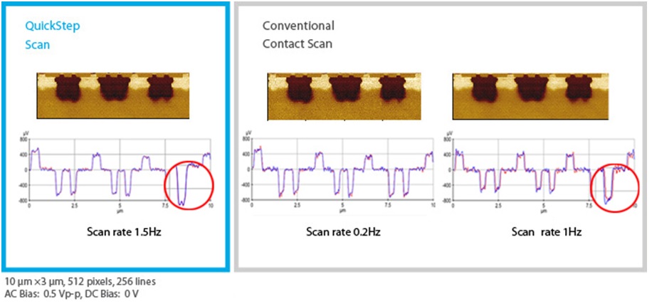
In order to improve the signal-to-noise ratio, conventional SCM adopts very slow scan speeds as a means of giving the detector enough time to collect data. QuickStep Scan differs from conventional methodology of slow continuous movement. Here, XY scanner stops at each pixel point to record the data and then makes a fast and rapid hop to the next measurement points. This effectively speeds up the scan rate while maintaining the same signal sensitivity of the measurements by conventional SCM at slow scan speeds.

Conventional SCM starts to lose the signal integrity as the scan rate increases, evidenced by the divergence between forward and backward scan signal. The QuickStep SCM maintains the same signal sensitivity as that of slow moving conventional SCM despite scanning at 5~10 times faster scan rates.
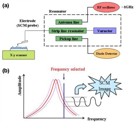
In addition, Park SCM is optimized for the best signal-to-noise ratio in the industry by selecting the optimal RF frequency that matches the doping range of sample, over a wide RF band from 600MHz to 2000MHz. From the resonance curve acquired one can maximize the resolution and sensitivity of the SCM probe by choosing the operating frequency which is at the maximum slope.
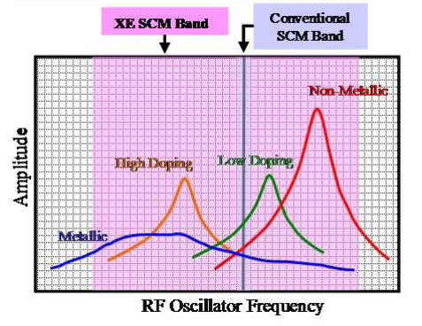
Even when using a very low AC bias voltages, Park SCM detector suppresses noise level and maintains a high signal-to-noise ratio, enough to tell the doping concentration less than an order of magnitude. This helps the semiconductor and device engineers perform failure analysis (FA) more accurately and efficiently with less effort and time.
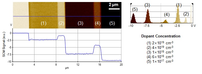
In short, QuickStep SCM is several times faster than conventional SCM, without sacrificing any measurement accuracy. It identifies causes of failure analysis, helps innovate the semiconductor design, and detects dopant concentration difference less than an order of magnitude.