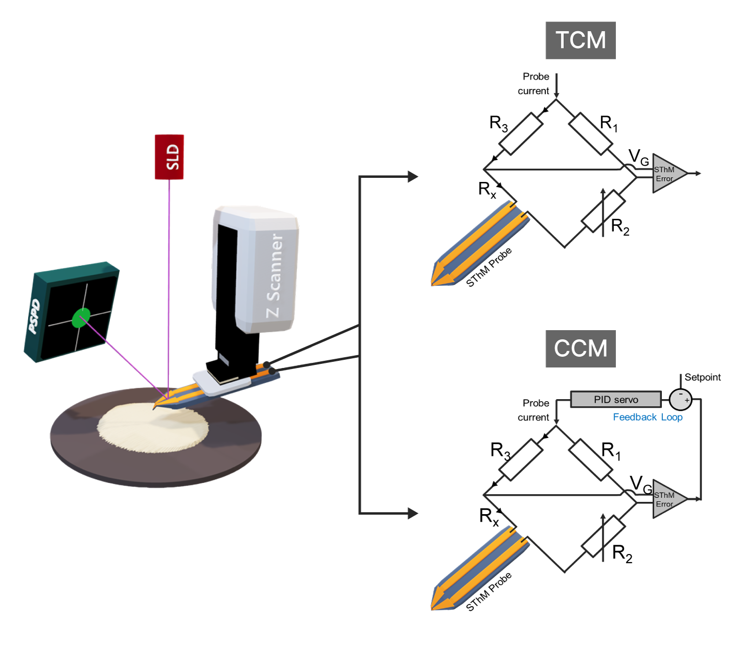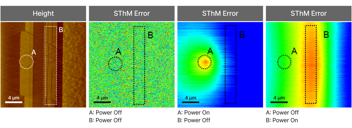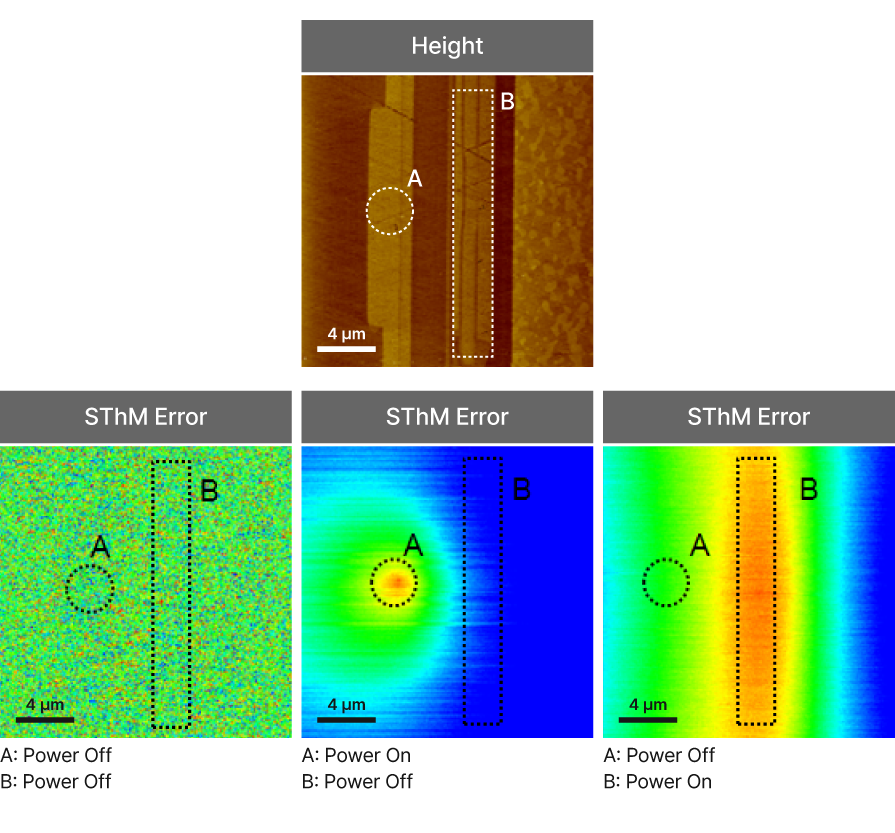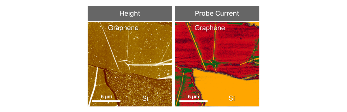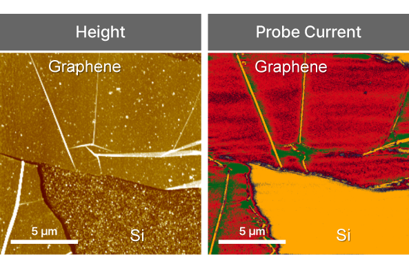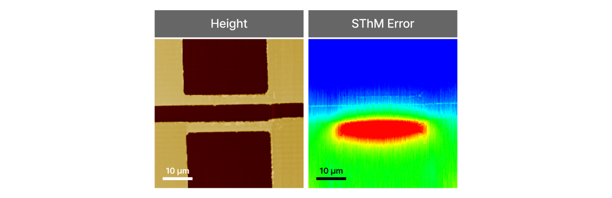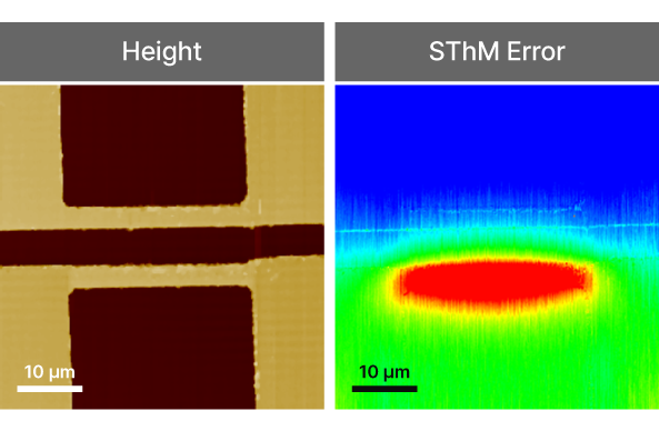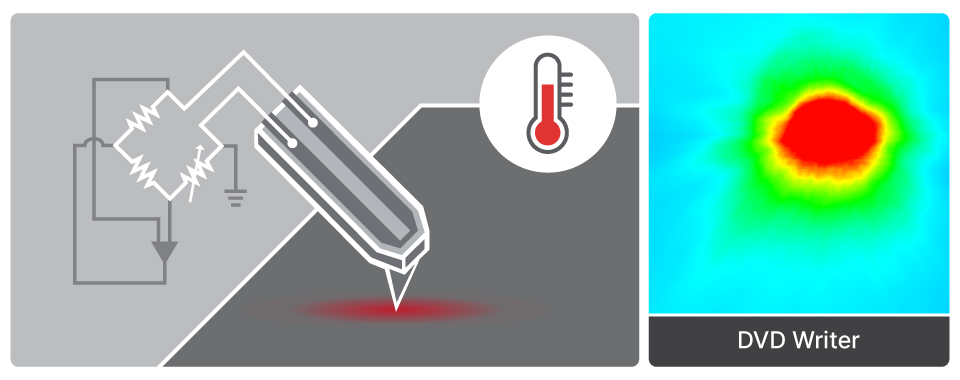
Scanning Thermal Microscopy
SThM
Thermal conductivity and temperature distribution imaging at the nanoscale using a nanothermal probe