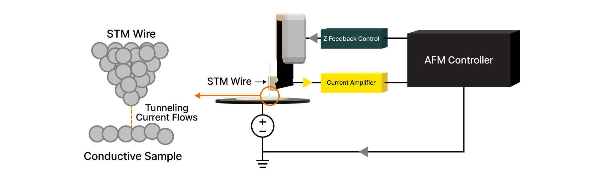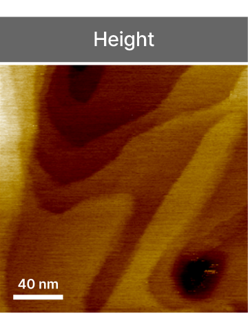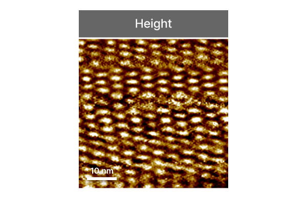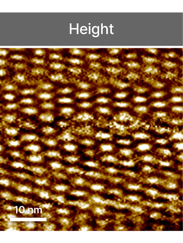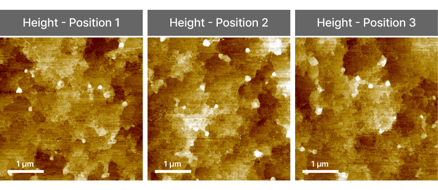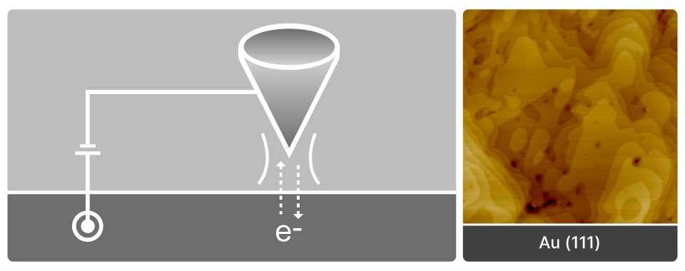
Scanning Tunneling Microscopy
STM
Atomic-scale electronic surface imaging based on tunneling current detection between tip and sample