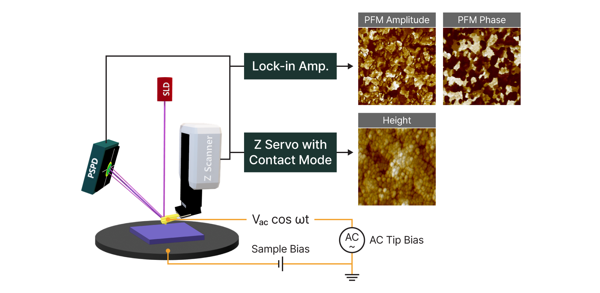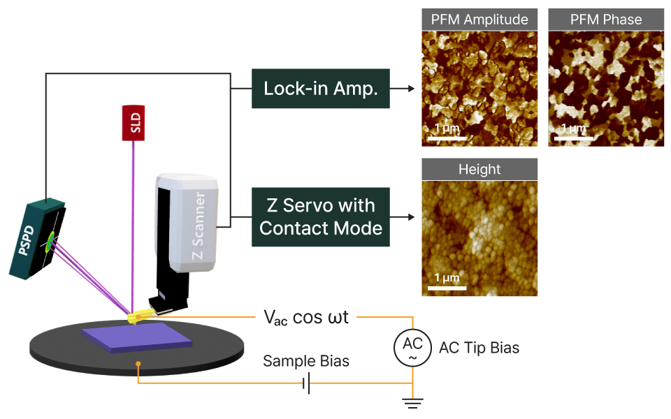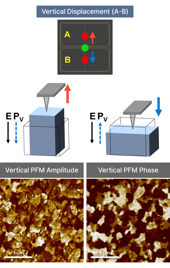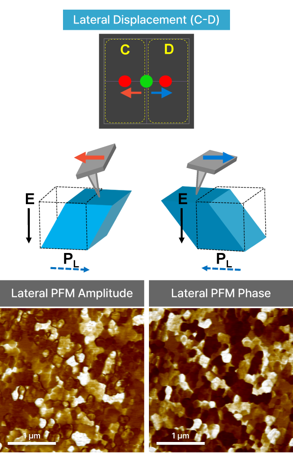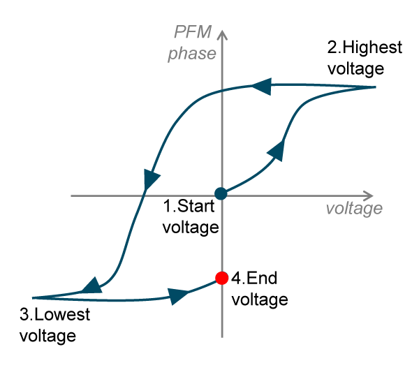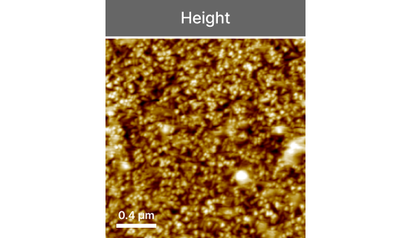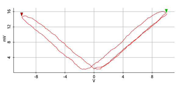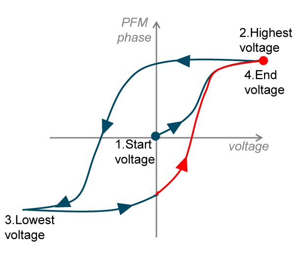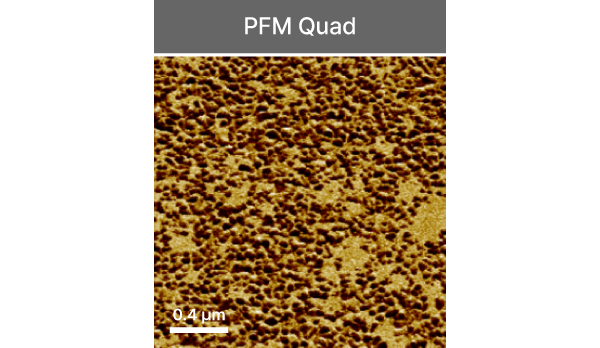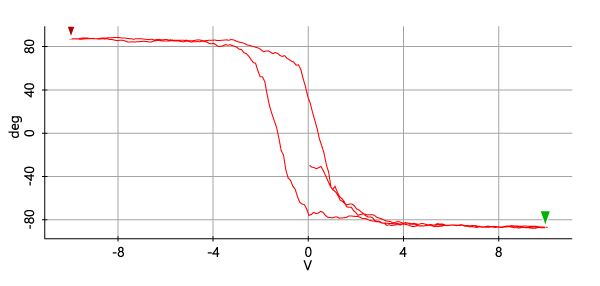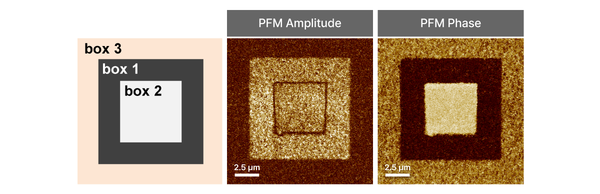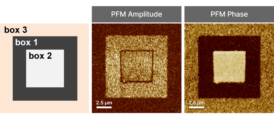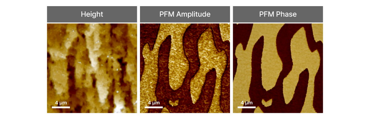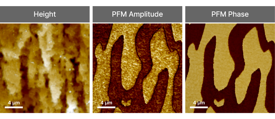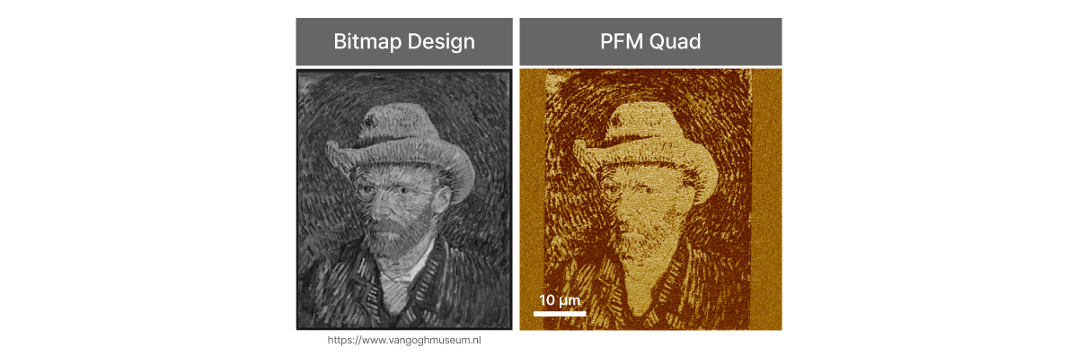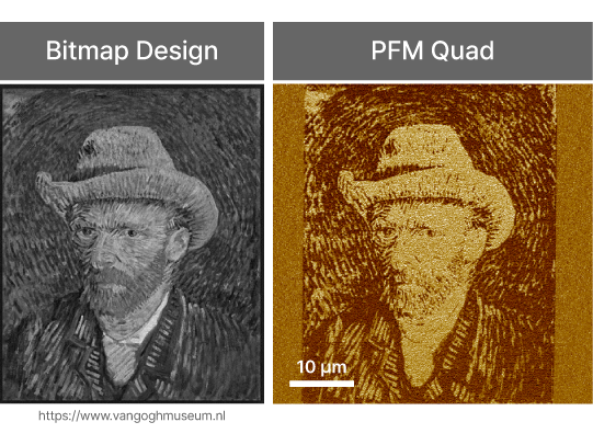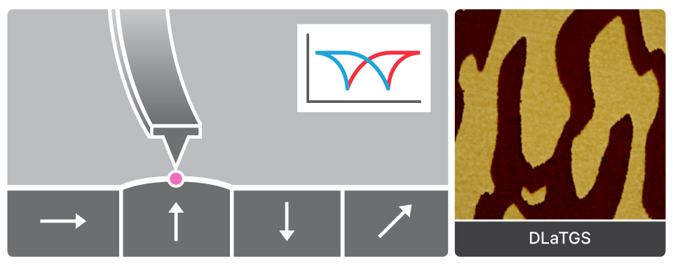
Piezoreponse Force Microscopy
PFM
Nanoscale ferroelectric and piezoelectric domain imaging through electromechanical coupling detection