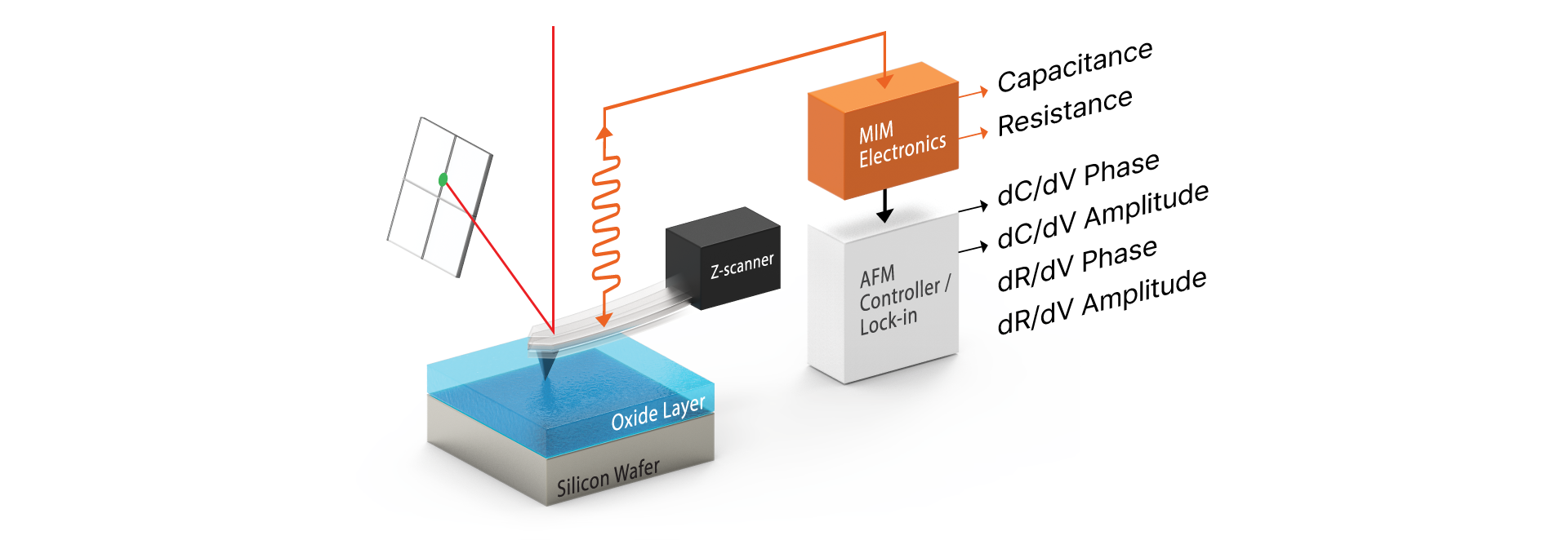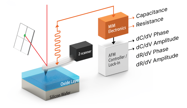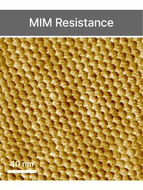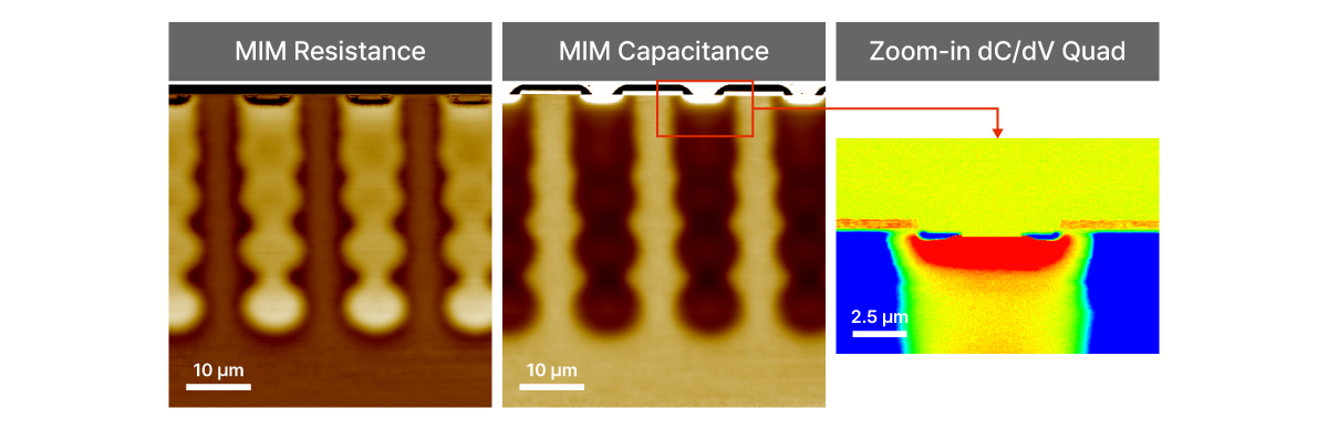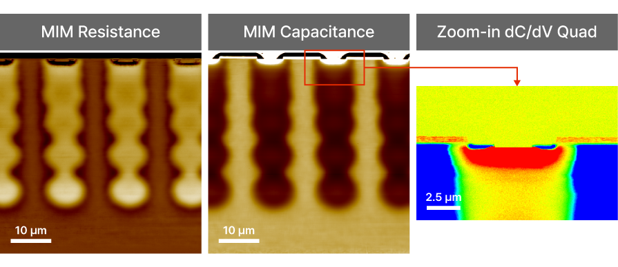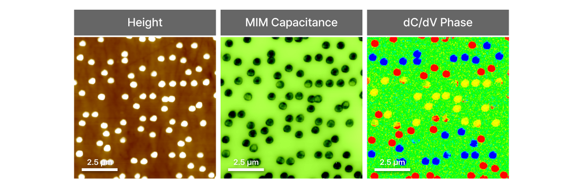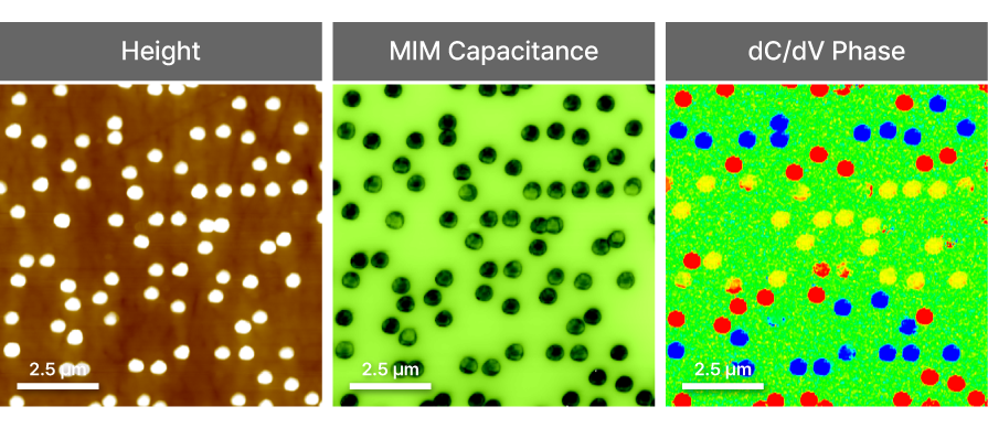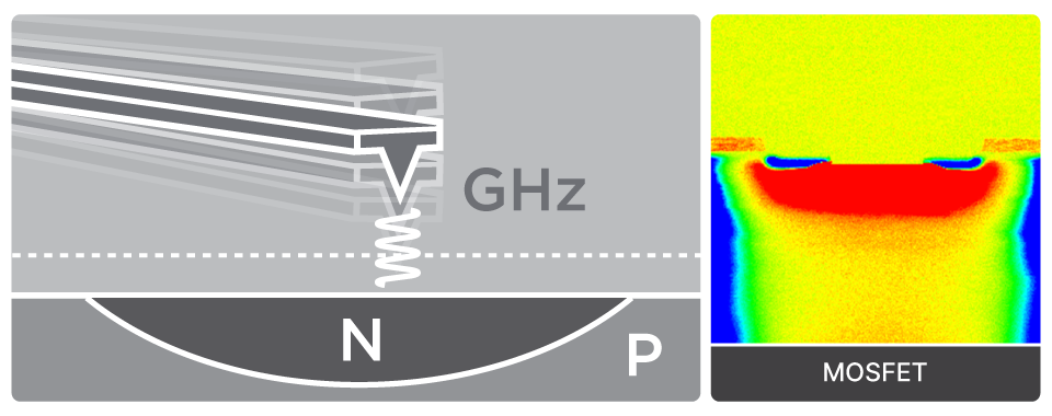
Microwave Impedance Microscopy
MIM
Nanoscale electrical property mapping based on capacitance and conductivity changes