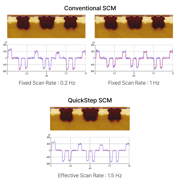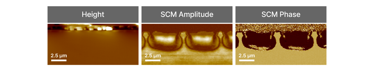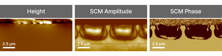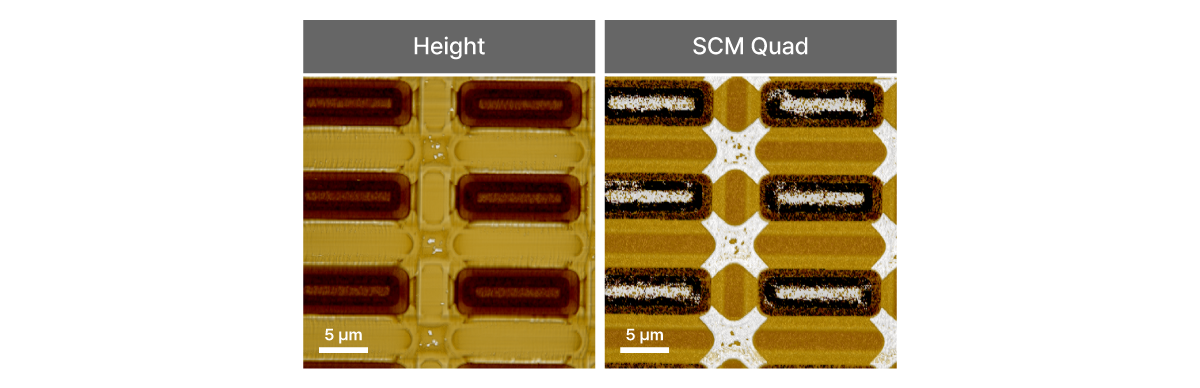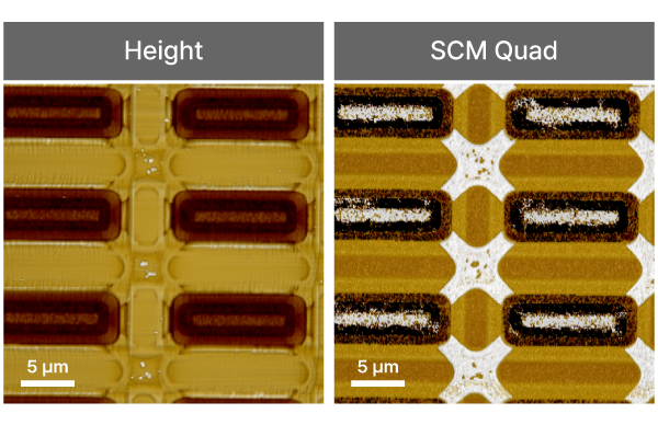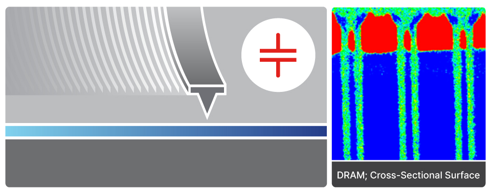
Scanning Capacitance Microscopy
SCM
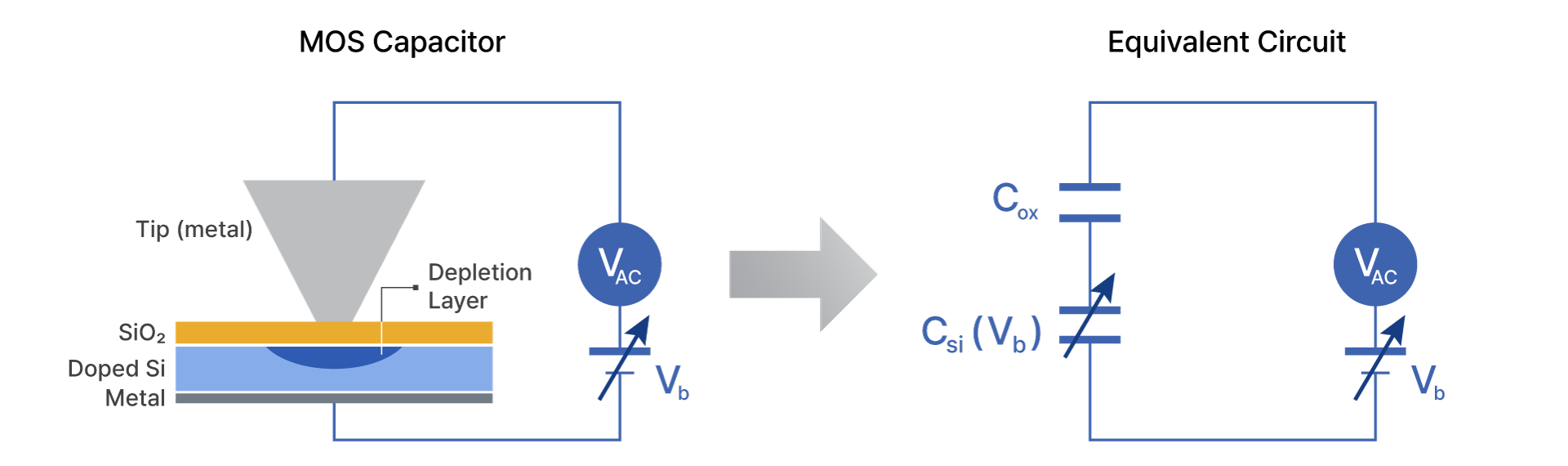
Nanoscale semiconductor doping and carrier profiling by detecting capacitance variations between the AFM tip and sample under AC bias