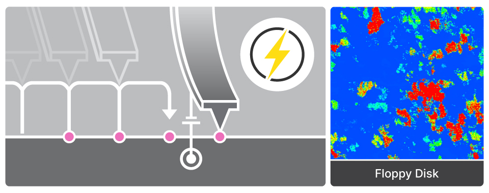
PinPoint™ Nanoelectrical mode measures precise electrical and mechanical properties at designated points, enabling detailed nanoscale material analysis with minimal lateral force.
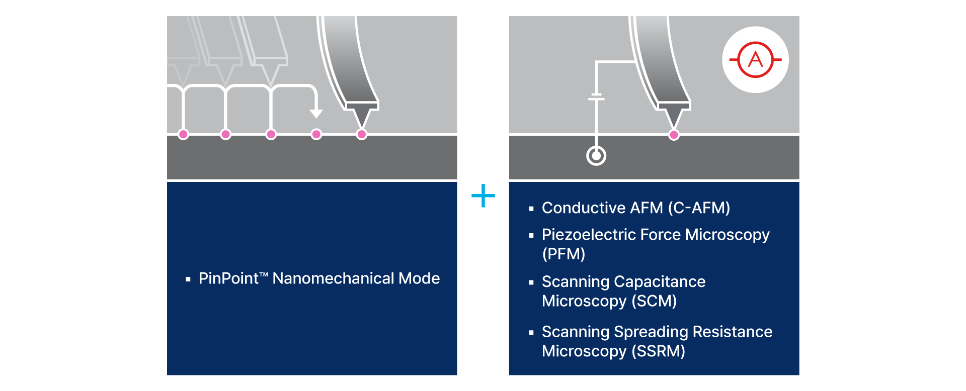
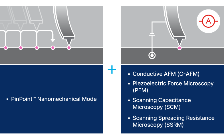
PinPoint™ Nanoelectrical mode acquires nanoscale quantitative data such as current (C-AFM), piezo response (PFM), capacitance (SCM), resistance (SSRM), and stiffness (PinPoint), all while simultaneously mapping surface topography. This method offers precise characterization across diverse materials by combining localized electrical sensing with mechanical property analysis. This approach eliminates lateral scanning during contact, greatly reducing tip wear and providing more stable electrical properties measurements, ideal for sensitive, delicate, uneven and heterogeneous samples without damaging the surface.
Reasons to Use This Mode
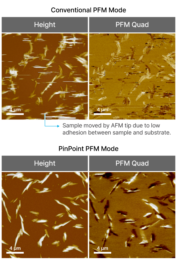
PinPoint™ Nanoelectrical mode minimizes lateral forces that cause sample and tip damage in conventional contact methods, enhancing measurement reliability and repeatability. It is particularly effective for analyzing soft, delicate, or heterogeneous materials such as soft polymers, polymer-based semiconductors and biological samples, where gentle, controlled interaction preserves surface integrity while delivering accurate nanoscale electrical and mechanical characterization.
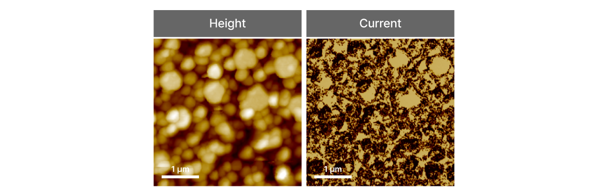
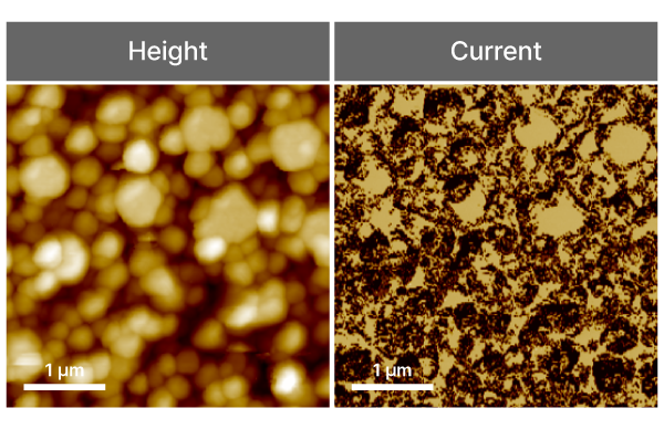
PinPoint™ C-AFM provides simultaneous, high-resolution mapping of both surface topography and current distribution in zinc oxide nano-rods, optimizing the detection of local conductivity variations by eliminating lateral tip-sample forces and enabling controlled contact force and time. This technique reveals critical correlations between nanorod diameter, morphology, and conductivity, offering quantitative insights inaccessible to traditional contact and tapping modes. It is ideal for sensitive nanostructures, as it ensures frictionless operation and preserves sample integrity during detailed electrical characterization.
Sample: Zinc Oxide Nano-rods
System: NX10
Scan Size: 4 µm × 4 µm
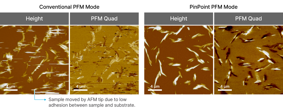
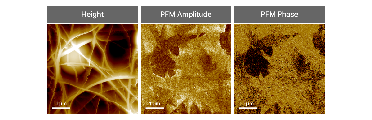
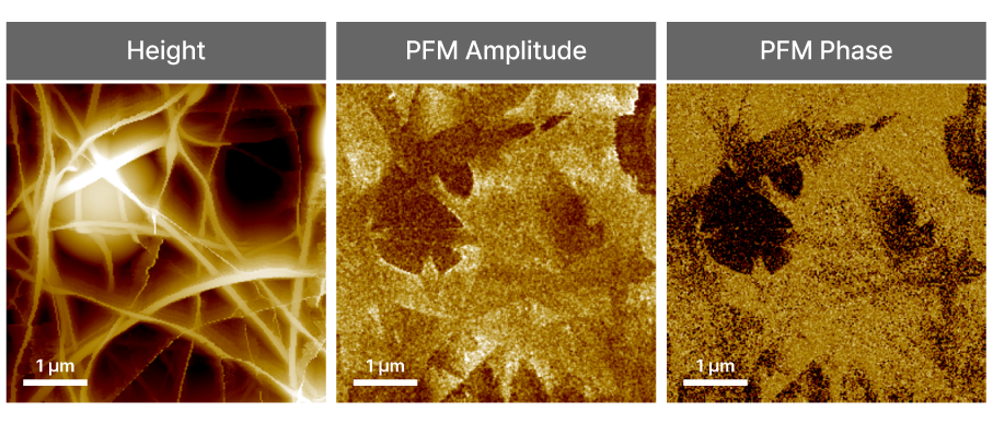
The PVDF fibrous membrane, with its soft and rough morphology, is ideal for PinPoint™ PFM. The AFM tip approaches the surface at each pixel, applies an AC bias to excite the sample’s electromechanical response, and collects amplitude and phase signals from the resulting cantilever deflection. It is a powerful tool for investigating functional materials such as ferroelectric thin films, piezoelectric nanostructures, and biological electromechanical systems under stable, repeatable measurement conditions.
Sample: PVDF Fibrous Membrane
System: NX10
Scan Size: 5 µm × 5 µm
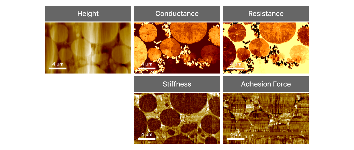
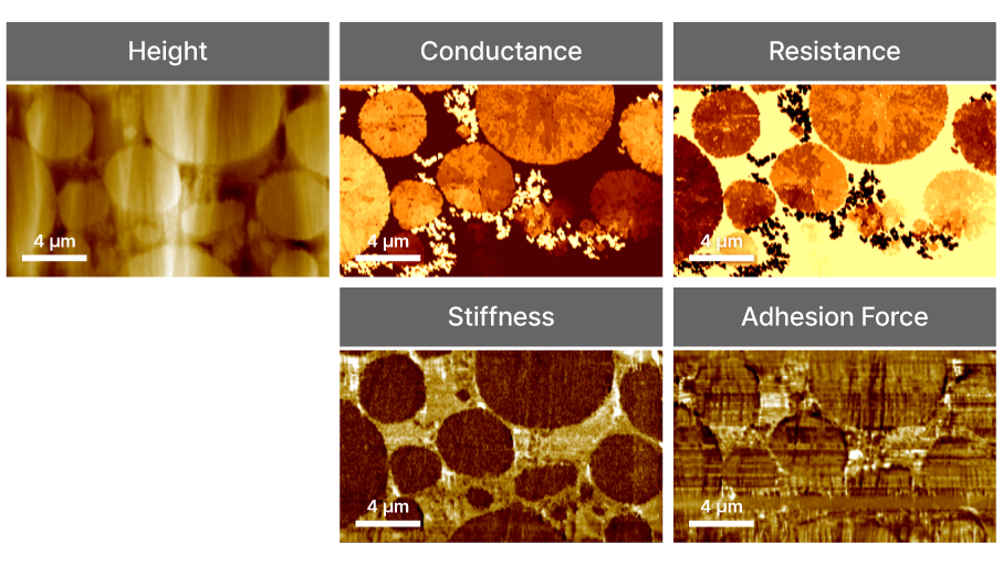
In PinPoint™ SSRM, using logarithmic amplification, the system detects current variations spanning several orders of magnitude, enabling carrier profiling across high/low doped regions. Combined with simultaneous force–distance data, this mode provides both mechanical and electrical information with nanometer resolution. Quantitative analysis of conductivity and stiffness at the nanometer scale provides crucial insights into electrode performance, aiding quality assessment and materials research for next-generation batteries.