Scanning Microwave Impedance Microscopy (sMIM)

Special Modes

Scanning Microwave Impedance Microscopy (sMIM)

Unlock the Power of sMIM to Advance Electrical Property Analysis for Scientific Research

What is sMIM?
Scanning Microwave Impedance Microscopy (sMIM) is an advanced technique that utilizes microwave reflections to analyze the localized electrical properties of materials with unprecedented precision. This innovative method allows researchers to study the relative permittivity and conductivity of samples with superior accuracy and sensitivity.
Key Features

High Signal-to-Noise Ratio & Sensitivity

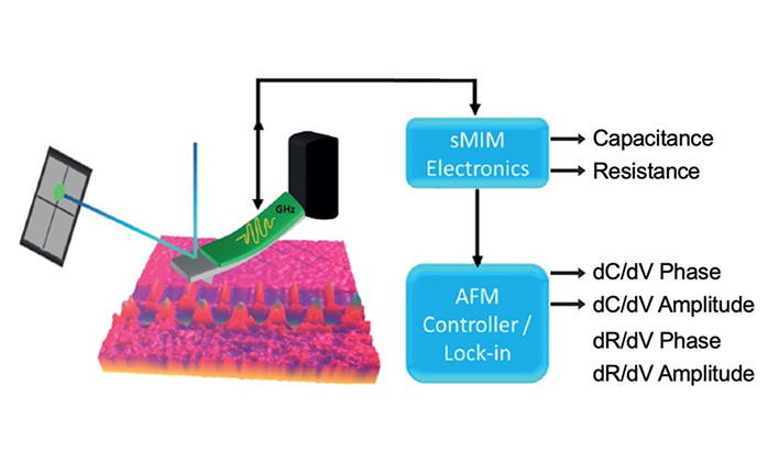
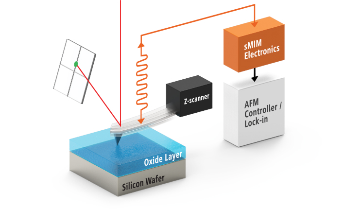
Utilizes ~3 GHz microwave frequency to deliver high-precision measurements.


Shielded Cantilever for Accuracy

Reduces stray coupling, ensuring data reliability.


High Lateral Resolution

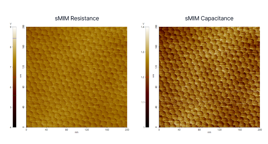
Provides detailed imaging of materials, ensuring accurate data acquisition.


No Electrical Contact to Sample

Requires no electrical connection to the sample, enabling the study of delicate and insulating materials.


Comprehensive Electrical Analysis

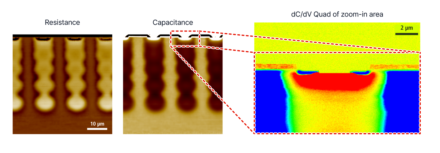
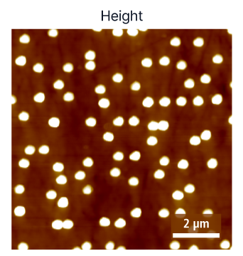
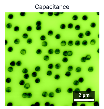
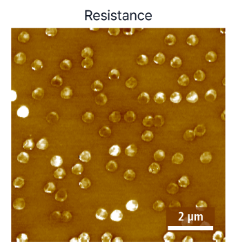
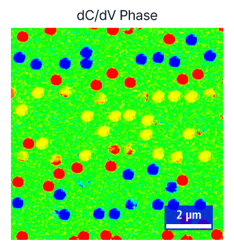
Measures dielectric constant, capacitance, resistivity, and dopant concentration.

Seamless Integration
Into Your Workflow
Park sMIM is designed for ease of use and efficient integration into existing research workflows. With intuitive software controls, straightforward probe handling, and minimal setup requirements, researchers can quickly implement sMIM without extensive retraining or reconfiguration. The non-contact nature of sMIM also eliminates the need for specialized sample preparation, saving time and preserving sample integrity. These advantages make Park sMIM a practical choice for both dedicated and shared research environments.
Differentiation from
Alternative Methods
Unlike traditional electrical measurement techniques, sMIM does not require physical electrical contact, reducing the risk of sample contamination and damage. Its ability to analyze electrical properties at the nanoscale with high sensitivity makes it superior to conventional capacitance or resistivity measurements.
Applications
Characterization of MOSFET

Characterization of PMOS, NMOS plug

Characterization tBG on hBN without electrode
What Applications Can Be Measured?

Semiconductors
  • Failure Analysis
  • Silicon on Insulator
  • E-Beam exposure characterization
Memory Device
  • Static RAM (SRAM)
  • Dynamic RAM (DRAM)
  • Erasable programmable read-only memory (E-PROM)
Dielectric Material
  • High-k Dielectrics
  • Silicon Nitride
  • Aluminum Oxide
2D Materials
  • Graphene
  • Hexagonal Boron Nitride (h-BN)